Zhang Yan, a PhD student of Professor Jiang Yang’s research group from School of Materials Science and Engineering, together with Dr. Yu Yongqiang from School of Electronic Science and Applied Physics, successfully fabricated a vertical multilayered n-MoS2/n-silicon homotype heterojunction for High-Speed Visible–Near-Infrared Photodetectors.
The work was published on Small, a renowned journal in materials science owned by Wiley, with the title of “In Situ Fabrication of Vertical Multilayered MoS2 /Si Homotype Heterojunction for High-Speed Visible–Near Infrared Photodetectors”, It was also reported by Materials Views China --Wiley’s website reviewing frontier materials science information and promoted on its Weibo account.
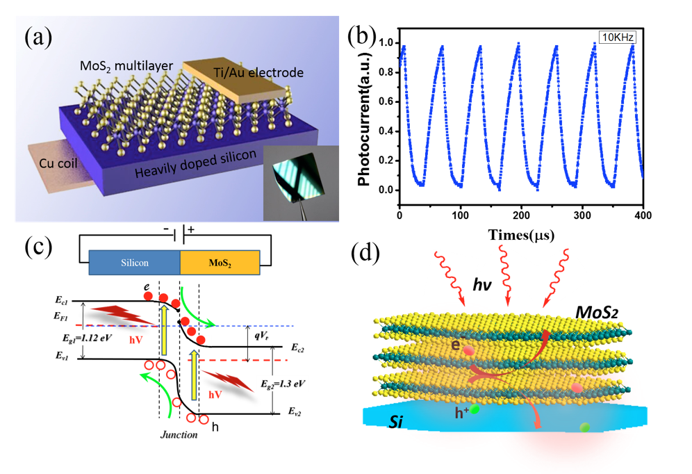
In recent years, the new-type 2D transition metal semiconductor materials, represented by MoS2, have aroused great interest from the public for its basic science researches and applications. MoS2, apart from its excellent graphite properties, embodies fine charge carrier mobility and absorption wavelength, and a band gap between 1.3-1.8 ev, which makes it potential for being a platform for new-generation photo-electronic parts. Photodetectors, as key components of the photo-electronic system, have a variety of applications in imaging technology, optical communication, and photonic IC.
In this work, a vertical multilayered n-MoS2/n-silicon homotype heterojunction is fabricated, which takes advantage of multilayered MoS2 grown in situ directly on plane silicon. Electrical characterization reveals that the resultant device exhibits high sensitivity to visible–near-infrared light with responsivity up to 11.9 A W–1. Notably, the photodetector shows high-speed response time of ≈30.5 µs/71.6 µs and capability to work under higher pulsed light irradiation approaching 100 kHz. The high response speed could be attributed to a good quality of the multilayer MoS2, as well as in situ device fabrication process. These findings suggest that the multilayered MoS2/Si homotype heterojunction have great potential application in the field of visible–near-infrared detection and might be used as elements for construction of high-speed integrated optoelectronic sensor circuitry.
Access to the paper:
http://onlinelibrary.wiley.com/doi/10.1002/smll.201502923/abstract
Access to the report:
http://www.materialsviewschina.com/2016/03/in-situ-preparation-of-multilayer-silicon-molybdenum-disulfide-high-speed-photodetectors/
Written by: Zhang Yan
Edited by: Wang Xiuqin
编辑:闵璇

 HOME
/
Content
HOME
/
Content